Low cost, Large Area and High quality GaN Substrate
Binary III-V direct bandgap semiconductor commonly used in light-emitting diodes
-
Wide bandgap material
-
Used to emit Blue/UV light
-
Can be operated at high temperature
-
High power electronics
-
High frequency transistors
Our Key technologies
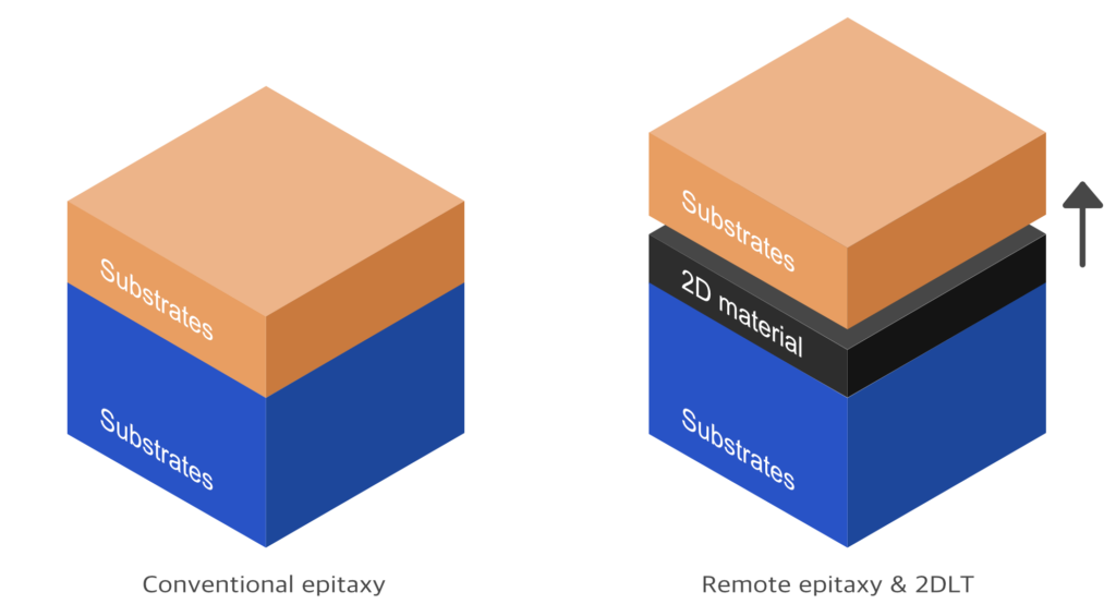
Remote Epitaxy & Two-dimensional material based layer transfer allows epitaxial growth on graphene and transferring to the host substrate. This technology gives Infinite reuse of parent wafer and fast layer release.
Remote epitaxy
Allow growing high-quality single crystalline semiconductor on graphene.
Two-dimensional Layer Transfer (2DLT)
Featured at the cover of Nature (2017)
Enable to lift-off and transfer thin-film to host substrate without degradation of the substrate.
Why Remote Epitaxy & 2DLT?
Fast layer release. Wafer surface protection. infinite reuse of parent wafer.

High-quality
Improvement of high quality of epitaxy over conventional epitaxy by being copied from substrates by remote epitaxy through 2D materials.
Easy Lift-off
Providing epilayers rapidly and easily removed from substrates by lift-off processing due to 2D materials.
Cost reduction
Significant cost reduction in view of preparation of epitaxy through the reuse of substrates due to lift-off processing.
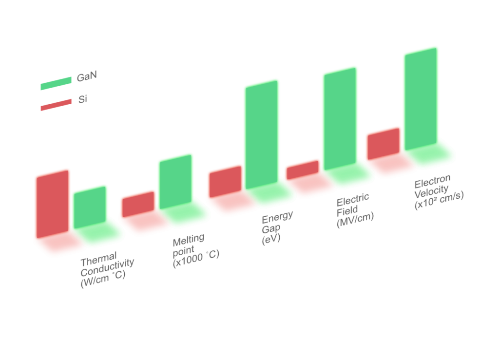
GaN is superior material
It is for high-performance devices
GaN is a superior material for Fast switching, Low on resistance, Less power needed, Less capacitance, and Smaller devices. Comparing with Si, GaN is good for high voltage operation, high frequency switching, and high temperature application.


