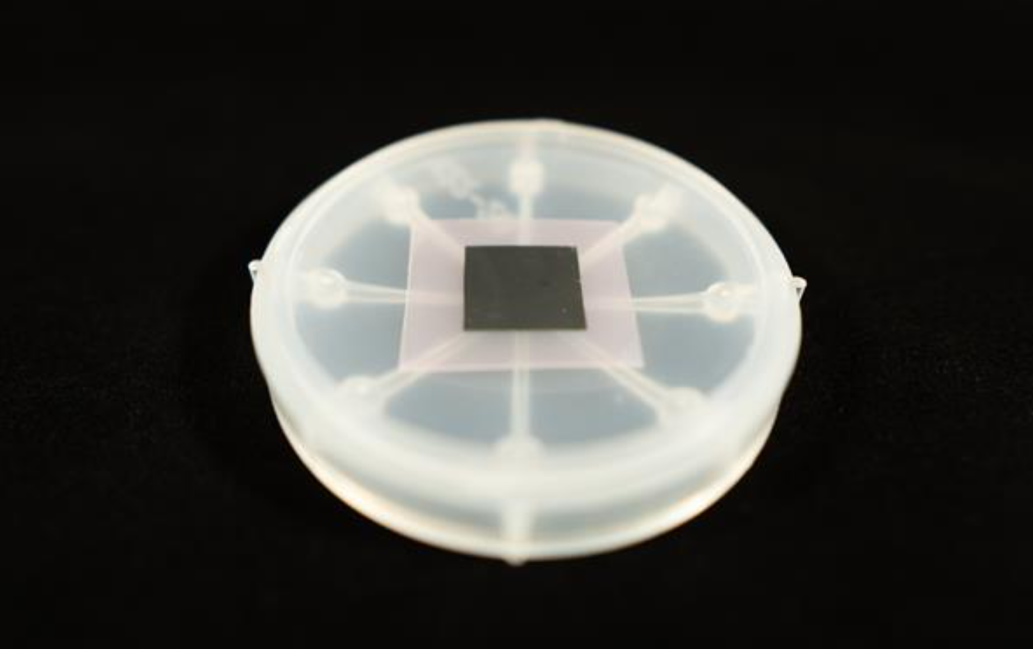
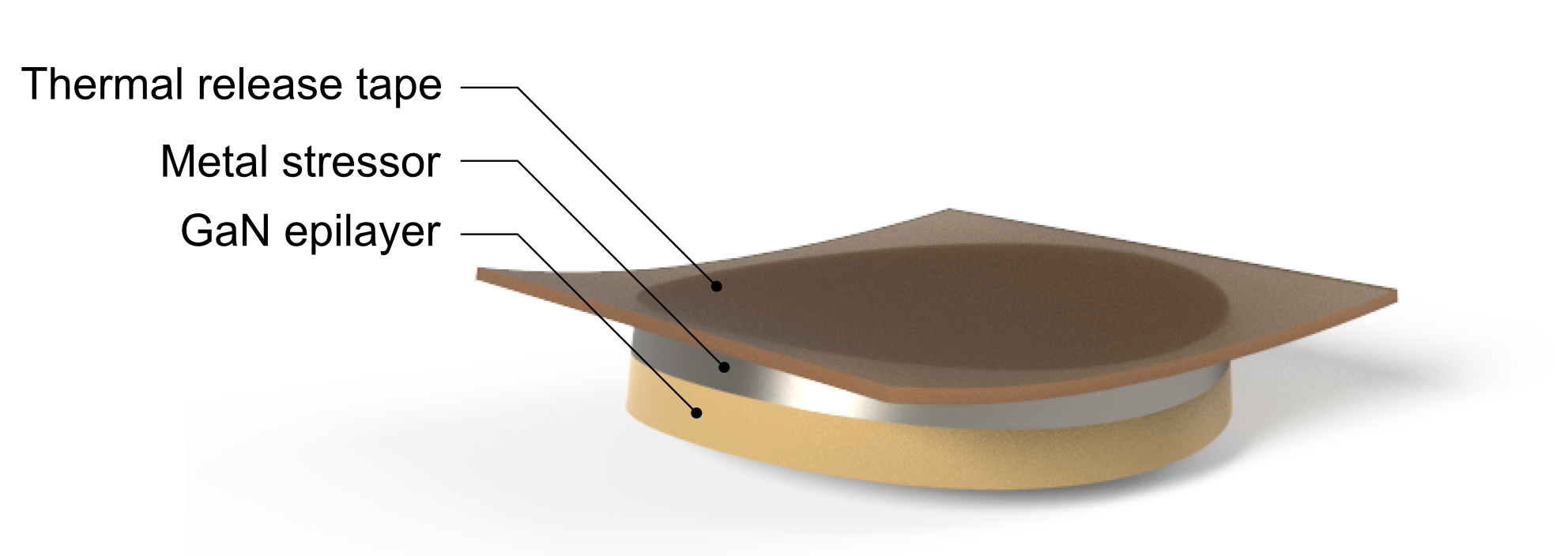
1. 2D-GaN Template
FSB 2D templates for Remote Epitaxy and 2 Dimensional Material based Layer Transfer (2DLT) are designed to facilitate a large area and high-quality single crystalline GaN epi-wafer for solution of high performance power and RF devices.
MBE based 2D templates with your GaN epitaxial growth can provide merits as follows;
- Large scale and high-quality GaN epi-wafer
- Lift off ready GaN epilayer
- Fast layer release (~ 1 sec) by 2D materials

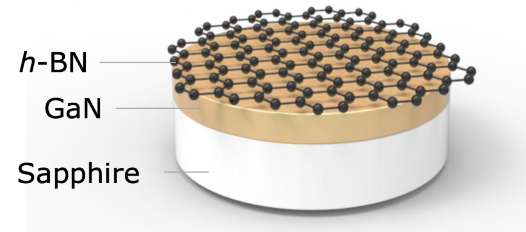
2. GaN on 2D template
FSB gallium nitride (GaN) templates designed by Remote Epitaxy and 2 Dimensional Material based Layer Transfer (2DLT) provide a large area and high-quality single crystalline GaN epi-wafer for solution of high performance power and RF devices.
MBE based GaN templates have several merits.
- Large scale and high-quality GaN epi-wafer
- Lift off ready GaN epilayer
- Fast layer release (~ 1 sec) by 2D materials
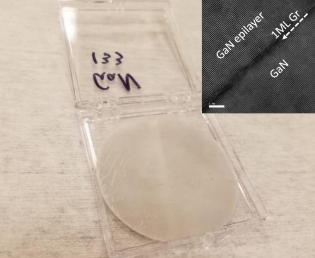
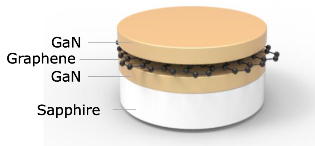
3. Free-standing GaN template
FSB free standing GaN by Remote Epitaxy and 2 Dimensional Material based Layer Transfer (2DLT) provides a large area and high-quality single crystalline GaN epi-wafer for solution of high performance power and RF devices.
MBE or MOCVD based free standing GaN can provide merits as follows
-
Large scale GaN epi-wafer
-
High-quality GaN epi-wafer
-
Production cost reduction due to low cost GaN epilayer
